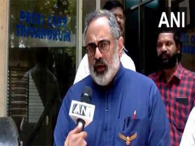
Union Minister for Electronics and IT, Shri Ashwini Vaishnaw, inaugurated two advanced Renesas design centers in Noida and Bengaluru, marking India’s entry into the elite 3 nanometer chip design space. This development positions India at the cutting edge of global semiconductor innovation, moving beyond previous 7nm and 5nm achievements.
Uttar Pradesh Emerges as a Semiconductor Powerhouse
The new semiconductor design centre in Uttar Pradesh is a key component of India’s comprehensive semiconductor strategy. This strategy spans design, fabrication, testing, and full supply chain integration. The move aims to unlock talent across India and decentralize innovation from traditional tech hubs.
Strengthening Talent Through Learning Kits and EDA Tools
To fuel long-term semiconductor growth, the Minister launched a new semiconductor learning kit. Over 270 academic institutions already equipped with advanced EDA software will now receive hands-on hardware kits. This dual approach of combining software with hardware learning is set to produce industry-ready engineers and strengthen India’s design capabilities.
Government’s Vision Aligned With Aatmanirbhar Bharat
Minister Vaishnaw credited Prime Minister Narendra Modi for prioritizing semiconductors under the Aatmanirbhar Bharat mission. He highlighted the rising demand for chips across electronics, healthcare, defense, and automotive sectors, underscoring the importance of timely infrastructure development and policy support.
Renesas Reaffirms Commitment to India’s Semiconductor Mission
Renesas CEO Hidetoshi Shibata praised India’s strategic importance in global semiconductor supply chains. He emphasized the company’s goal to support startups, academic institutions, and expand design-to-testing capabilities through initiatives like the Chips to Startup Programme and the DLI Scheme. The company’s expanded footprint in Noida, Bengaluru, and Hyderabad reflects its commitment to India’s talent and innovation potential.
This landmark step not only elevates India’s role in semiconductor design but also cements its ambition to be a self-reliant, global tech manufacturing hub.


